I as tech guy, like to know how existing tech works. Pimax 8K V1-V3 is existing tech, so not pure speculation(marketing). So you know difference between my specs and Pimax specs(envisioned product specs vs specs derived from existing product in prototype stage). Here is my tech overview of tech used in existing products at V2 and V3 stage as demo footage proves.
Agree or disagree, not for lay men, requires understanding of DSC, panel/driver IC/HW understanding (educational background preferred). Here it comes:
Pimax “8K” prototype stage tech analysis:
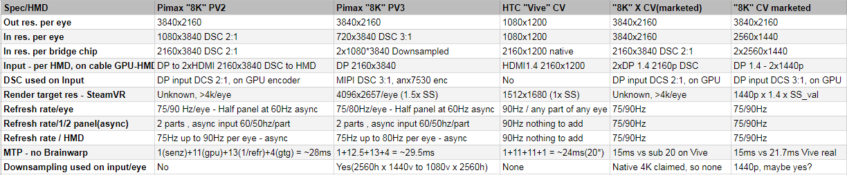
Single " 4K panel specs* " : We have CLPL holder that is containing 4 slices of screens, 4K panel is made by taking 4 1920x1080p panels tilted 90degrees, and cut in half on (920h x 1080v x 4) is actually “4K panel”. And each slice, has its own backlight, that through firmware update can be made to produce strobbing effect, that will mask ~4ms GTG pixel response time of single slice(Low persistence effect). This is SW upgrade that Valve is referring to when claims LCD is “good enough” for high end VR now. Now, lets inspect the connections per CLPL holder that contains driver IC.
"Driver IC specs* ": Pimax SW engineer, pointed out some limitation of Driver IC regarding to input on MIPI-DSI ports. If we feed native signal to 4x1K panel(4K from now on), we are limited to 3840x2160p@30 interleaved to 60. So actual refresh rate, when transferring native input res is 30Hz/slice limit, 60Hz/2 slices(if input is 30hz interleaved, not optimal for VR use), or 120Hz/4 slices. We use technique called “interlacing” to achieve double perceived refresh rate. About interlacing check John Carmack remark on interlaced displays. I derive from this that Pimax wants to push this idea to reality. That is how you get brainwarp numbers like 150-180, that is refresh rate not of (whole)display, but rate at which 2 slices(2x1K) b-light is on, so per 2K slice we get 150(75+75)-180(90+90) sync backlight on/off rate, we have 1 MIPI per 2K slice, and that is how Pimax gets confidence to put that number on Brainwarp specs in refresh rate specs. This is confusing to lay people, since they don’t know as much as engineer who wrote 150-180 on some spec sheet(without * next to it). Marketing team is using this number not in user friendly way, I criticize Pimax for that(I am pro-truth not pro-_any_company). To get real benefits from this approach we need to use at least 1MIPI port per 2K slice, at native res(4k) input. For interlacing effect not interleaving effect. And to go from 30(original num) to 60Hz(i*) i* - interlaced pixels mode. This is why Pimax advertise with 4K HMD, real deal 60Hz(up to 90 async), to achieve it they use shutter to sync(to eyes) the 90async/2K slice refresh rate. You get downside, loss of brightness(as reported), comparing to native 60Hz(with 60Hz/whole panel sync b-light). I don’t know specs of the each 1k x 1k slice(panel) but CLPL holder I think uses same Driver IC as with 4K HMD in 8K with updated firmware to get real CLPL(not simulated with shutters).
That is why we get /eye in current marketed tech specs of 8K CV.
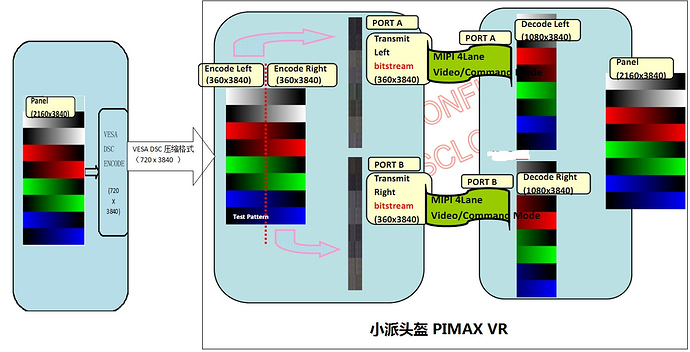
About actual input per 2K slice, this is also problematic. Driver IC has specs* to support DSC 1.1 version/FBC - Qualcomm similar tech to (de)compress the signal from MIPI to actual individual 1K panels/slices. To feed in more than 30Hz input(what is limit per 4K panel), by using same number of MIPI per 2K slice, Pimax uses two techniques. In 4K HMD, uses actual Driver IC as upscaler, this is famous “scaler chip” in fact is just IC put in front of the CLPL holder. So they use same tech 2x. BTW designing custom IC(ASIC) is cost effective in 1M+ units, so I don’t criticize Pimax for this move. What I criticize is that they are hiding behind 1.4b bandwidth limits, to use as excuse why Pimax 4K HMD can’t have 90Hz input like Rift/Vive. Real reason is, Driver IC needs DSC signal(to feed the panel higher than 60Hz input). They take HMD signal with 4:2:0(pixel compression), feed it into “DSC (en/de)coder IC/marketed as scaler”. So throught cable they send 2160v x3840h(4:2:0)@60 signal for both eyes to Driver IC used as scaler, because it doesn’t get native 4K, but compressed(on PC side, (up)down-scaled, (up)down-sampled w/e) 2x2560h x 1440v formated for “DSC 3:1 input per 2K slice” (360x3840) (after real DSC treatment) and 1080v x 3840h per eye, after 2:1 encoding. So input per “scaler” is 2x1080v x 3840h with 16b/pixel color(4:2:0). Data flow: 2x2560hx1440v(GPU render target, no SS) - 2x1080v x 2160h(down/upscaling on Pimax post-render pipeline) - 2160v x 1080h RGB6@60 (data through 1xHDMI 1.4 to HMD) - 1080h x 3840v DSC 2:1 (DSC encoder/scaler in Pimax words) - fed to 360x3840(DSC 3:1) input to DSC decoder on CLPL holder/4K panel holder/driver.
How many steps, 1,2,3,4,5 complicated for people who haven’t used algorithms before  . I get that, but marketing render target as input res is misleading at best.
With 8K V2, actually used is different (smarter approach), not perform (down)upscaling on PC, but use GPU DSC engine to feed the CLPL holder with DSC 2:1 signal, if use 1 MIPI ports 2K slice, or DSC 3:1 if use DSC 2:1 with 1 MIPI per 2x 2K slices.
How they used actually GPU DSC engine, on V1-V2, vs using “fake DSC process” in P_4K and P_V3.
Here are components of 8K V1-V2:*
1x DP 1.4 to 2xHDMI splitter, unknown maker(performs almost no logic).
2x HDMI to DisplayPort Bridge Controller ANX7678, in specs noted it is designed for use with ANX7530. Specs.
2x ANX7530 . Used to accept out from anx7678(2160v x3840h (DSC 2:1)) and sent to MIPI, actual DSC(real deal, used Algorithm not just math to reduce BW) to each MIPI 1080v x 1920h, 2MIPI per eye, so we get not uspcaled, but decompressed 4K per eye output res. Not native, but decoded/decompressed/restored res. Much better than dumb upscaling.
Why this method won’t work with 1xDP and direct DP to anx7530, because anx7530 is not designed for native DSC 1.4, but to be fed via anx7678, then the claim DP 1.4 compatible have sense. This guys design HW they are correct always or HW is junk.
That is why I write we got migration from "8K V1-V2 X P"prototypes, that are shown on Public demo, to V3 that is “8K V1 P” that is shown to have 90Hz input probs, uses upscaling vs DSC etc etc. From 4K upscale to 8K, input become in marketing data, 2x2560x1440. Same BS as with 4K HMD.
Debunked or not, make your call.
*- unofficial specs, reverse engineering used. (common practice), not pure speculation as some pro-Pimax people claim. On KS projects you can do pure speculation on specs, aka marketing specs, as I note in my specs sheet(top post).
Goal: Get Pimax to understand backers will not be happy if get same experience as with 4K, only better tracking in double FOV with same input res as half FOV res. Or give backers option, 2xHDMI with short cables (for use like PSVR but with good head/motion tracking). But no roomscale. Or give option to wait for DSC 2:1(real DP 1.4 input), and room scale, expected at date as “8K X” ship date.
If solution DP1.4-2xHDMI to 2x anx7530 is too expensive. Give option to trade all rewards for actual DP1.4 to b/o box, to 2x anx7530. I think most backers will decide, if want to wait for rewards, or wait for product as was shown to public and they think they backed.
Give backers options, if can’t solve DSC on DP input without using HDMI and B/O box.
Option 1: Trade all rewards for “8K V2 CV” HMD, to get same experience as “8K V2 P”, 1920x2160/eye(after DSC 3:1 compression) restored to to 4K resolution, not simply upscaled, that is non tech correct for DSC algo to call it. This is same as 8K X, but in upscale mode, but on horizontal res, like Checkerboard rendering, so not so simple as divide/multiply Res. Proper Mid gen VR product. With maybe 2nd gen FOV, this is speculation/assumption ofc, I can’t know specs of future products that are not marketed!
If possible with GPU out DSC encoded 4K to HMD directly(SW encoder), if not, use B/O box(DP 1.4 to 1xHDMI 2.0), trade some KS reward for it.
Option 2: Get “8K V3 CV” HMD with 2x2560x1440 target render res, ASAP. Wait for rewards. Expect nVidia/Pimax to provide SW DSC encoding solution at later date, to give promised product specs. Probably no ETA from Pimax possible, heard there were plans nVidia wants to retrofit DP 1.2 cards with DSC capability… Rumors to be clear.
I am pro-backers, for some reason I prefer to defend people from companies, than companies from people xD.
TL:DR
Sorry can’t perform Fake DSC, it would lose valuable data(display bad picture about my reverse engineering skills) .
This is in depth explanation of my logic, without all sources, cause it would be huge time consumer to explain every tech detail in my logic. This is digest version, imagine amount of data I have in head if this is DSC 10:1 to it . If you want lay-man version, console tech analogy, read this.

 .
.
